 VIPSolutions
Q1) Tn the cirenik below, the source ond drain ac vo tinges ave held ot ground . Denve an enpression for fr. (Bonus: 10 points) Ceo oy 1 tout i, + Ces The hreueny ob which, the went gain of the MOS device drops Ho 1, Js called he“ Teamsit Frequacy” BL Ta = =) N——r—C— TT
Question:
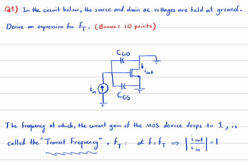 Q1) Tn the cirenik below, the source ond drain ac vo tinges ave held ot ground .
Denve an enpression for fr. (Bonus: 10 points)
Ceo
oy 1
tout
i, +
Ces
The hreueny ob which, the went gain of the MOS device drops Ho 1, Js
called he“ Teamsit Frequacy” BL Ta = =)
N——r—C— TT
This is AI generated Response.
Asked by: ABCD
Created at: 2025-09-17 13:01:52
Asked by: ABCD
Created at: 2025-09-17 13:01:52
Final Answer:
Rendered
Raw Text
Did you like this answer?
Let's break down and solve the problem step by step:
## **Given:**
- **Circuit:** Source and drain are **AC grounded**.
- **Components:** Two capacitances, \( C_{GS} \) (gate-source) and \( C_{GD} \) (gate-drain).
- **Input:** \( i_{in} \) is injected at the gate.
- **Output:** \( i_{out} \) is taken from the source (which is also AC grounded).
- **Definition:** Transit frequency (\( f_T \)) is the frequency at which the current gain drops to 1:
\[
\left| \frac{i_{out}}{i_{in}} \right| = 1 \quad \text{at} \quad f = f_T
\]
---
## **Step 1: Small-Signal Equivalent Circuit**
For this configuration, the small-signal model at high frequencies is dominated by the gate-source and gate-drain capacitances. The **source** and **drain** are both AC grounded.
- The input current \( i_{in} \) splits between \( C_{GS} \) and \( C_{GD} \).
---
## **Step 2: Current Division**
### **Impedance of Capacitances:**
\[
Z_{C_{GS}} = \frac{1}{j\omega C_{GS}}, \quad Z_{C_{GD}} = \frac{1}{j\omega C_{GD}}
\]
### **Current through \( C_{GS} \):**
The total input current \( i_{in} \) splits between \( C_{GS} \) and \( C_{GD} \) (both to ground):
\[
i_{out} = \text{current through } C_{GS} = i_{in} \frac{Z_{C_{GD}}}{Z_{C_{GS}} + Z_{C_{GD}}}
\]
But since both capacitors are to ground and in parallel, the current division is:
\[
i_{in} = i_{GS} + i_{GD}
\]
\[
i_{GS} = \frac{C_{GS}}{C_{GS} + C_{GD}} i_{in}
\]
\[
i_{GD} = \frac{C_{GD}}{C_{GS} + C_{GD}} i_{in}
\]
But **transconductance (\( g_m \))** comes into play: The output current is \( i_{out} = g_m v_{gs} \).
---
## **Step 3: Relating Input Current to Gate-Source Voltage**
\[
i_{in} = (j \omega C_{GS} + j \omega C_{GD}) v_{gs}
\]
\[
i_{in} = j \omega (C_{GS} + C_{GD}) v_{gs}
\]
\[
v_{gs} = \frac{i_{in}}{j \omega (C_{GS} + C_{GD})}
\]
---
## **Step 4: Output Current**
\[
i_{out} = g_m v_{gs} = g_m \left( \frac{i_{in}}{j \omega (C_{GS} + C_{GD})} \right)
\]
---
## **Step 5: Current Gain**
\[
\frac{i_{out}}{i_{in}} = \frac{g_m}{j \omega (C_{GS} + C_{GD})}
\]
Magnitude:
\[
\left| \frac{i_{out}}{i_{in}} \right| = \frac{g_m}{\omega (C_{GS} + C_{GD})}
\]
---
## **Step 6: Solve for Transit Frequency (\( f_T \))**
At \( f = f_T \):
\[
\left| \frac{i_{out}}{i_{in}} \right| = 1
\]
\[
\frac{g_m}{2\pi f_T (C_{GS} + C_{GD})} = 1
\]
\[
f_T = \frac{g_m}{2\pi (C_{GS} + C_{GD})}
\]
---
## **Final Expression:**
\[
\boxed{
f_T = \frac{g_m}{2\pi (C_{GS} + C_{GD})}
}
\]
---
### **Summary Table**
| Parameter | Expression |
|--------------------|-----------------------------------|
| Transit Frequency | \( f_T = \frac{g_m}{2\pi (C_{GS} + C_{GD})} \) |
**This is the required expression for the MOSFET transit frequency (\( f_T \)) for the given circuit.**
📢 Instructions:
- Ask anything relatd to above question only.
- For new Question goto :