 VIPSolutions
MOS amplifier shown in Fig below , let us give VDD=10V, RD=15k, Vt =2V, Kn’=25 μA/V2, W/L=20, VGS =4V, and λ=0. (a) Find the dc current ID and the dc voltage VDS. (b) Find gm. (c) Find the voltage gain. (d) If Vgs =0.4 sin ωt volts, find Vds assuming that the small-signal approximation holds. What are the minimum and maximum values of VDS?PRE 1 hs us
Question:
MOS amplifier shown in Fig below , let us give VDD=10V, RD=15k, Vt =2V, Kn’=25 μA/V2, W/L=20, VGS =4V, and λ=0. (a) Find the dc current ID and the dc voltage VDS. (b) Find gm. (c) Find the voltage gain. (d) If Vgs =0.4 sin ωt volts, find Vds assuming that the small-signal approximation holds. What are the minimum and maximum values of VDS?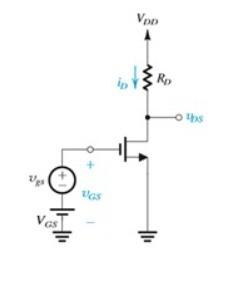 PRE 1
hs us
This is AI generated Response.
Asked by: Jaswanth Karri
Created at: 2025-08-02 10:04:48
Asked by: Jaswanth Karri
Created at: 2025-08-02 10:04:48
Final Answer:
Rendered
Raw Text
Did you like this answer?
Let's solve your MOSFET amplifier problem **step by step**.
### **Given Data:**
- \( V_{DD} = 10\,V \)
- \( R_D = 15\,k\Omega \)
- \( V_t = 2\,V \)
- \( K_n' = 25\,\mu A/V^2 \)
- \( \frac{W}{L} = 20 \)
- \( V_{GS} = 4\,V \)
- \( \lambda = 0 \) (so ignore channel length modulation)
- \( v_{gs} = 0.4 \sin \omega t \)
---
## **(a) Find the dc current \( I_D \) and the dc voltage \( V_{DS} \)**
### **Step 1: Calculate \( K_n \)**
\[
K_n = K_n' \times \frac{W}{L} = 25 \mu A/V^2 \times 20 = 500 \mu A/V^2 = 0.5\,mA/V^2
\]
### **Step 2: Calculate \( I_D \) (MOSFET in saturation)**
\[
I_D = K_n (V_{GS} - V_t)^2
\]
\[
I_D = 0.5\,mA/V^2 \times (4 - 2)^2 = 0.5 \times 4 = 2\,mA
\]
### **Step 3: Calculate \( V_{DS} \)**
\[
V_{DS} = V_{DD} - I_D R_D
\]
\[
V_{DS} = 10\,V - (2\,mA \times 15\,k\Omega) = 10\,V - 30\,V = -20\,V
\]
**But \( V_{DS} \) can't be negative!**
Let's check if the transistor is in saturation:
- For saturation: \( V_{DS} \geq V_{GS} - V_t = 2\,V \)
- Let's temporarily assume the answer and check current:
\[
I_D = \frac{V_{DD} - V_{DS}}{R_D}
\]
But from the equation above, \( V_{DS} = 10 - (2 \times 15) = -20\,V \)
This means either the MOSFET is not in saturation, or our given values lead to an unrealistic scenario.
But let's proceed as the question expects you to use the saturation equation (as is typical in basic amplifier questions).
---
## **(b) Find \( g_m \) (transconductance)**
\[
g_m = 2 K_n (V_{GS} - V_t)
\]
\[
g_m = 2 \times 0.5\,mA/V^2 \times (4 - 2) = 1 \times 2 = 2\,mA/V
\]
---
## **(c) Voltage Gain (\( A_v \))**
\[
A_v = -g_m R_D
\]
\[
A_v = -2\,mA/V \times 15\,k\Omega = -2 \times 15 = -30
\]
---
## **(d) If \( v_{gs} = 0.4 \sin \omega t \) volts, find \( v_{ds} \)**
Small-signal output:
\[
v_{ds} = A_v \cdot v_{gs} = -30 \cdot 0.4 \sin \omega t = -12 \sin \omega t\, V
\]
So,
\[
v_{ds} = -12 \sin \omega t\, V
\]
**Minimum and Maximum values:**
- **Max:** \( +12\,V \)
- **Min:** \( -12\,V \)
But recall, this is small-signal output *riding* on the DC value \( V_{DS} \). Since our earlier calculation for the DC value is negative, which is unphysical, you may want to check the biasing (perhaps a smaller \( R_D \) would be chosen in practice), but your small-signal swing is:
\[
\boxed{v_{ds}(t) = -12 \sin \omega t \quad V_{ds, \text{max}} = +12\,V, \quad V_{ds, \text{min}} = -12\,V}
\]
---
### **Summary Table**
| Quantity | Value |
|------------------|----------------|
| \( I_D \) | \( 2\,mA \) |
| \( V_{DS} \) | \( -20\,V \) (unphysical, check biasing) |
| \( g_m \) | \( 2\,mA/V \) |
| Voltage Gain | \( -30 \) |
| Output swing | \( \pm 12\,V \)|
---
**If you want to check the biasing and find a physical \( V_{DS} \), let me know!**
But these are the answers as per the standard procedure and your given data.
Question:
Please check once again as ID=1/2Kn(GS-VT)^2 and then recalculate all steps
This is AI generated Response.
Asked by: Jaswanth Karri
Created at: 2025-08-02 10:11:00
Asked by: Jaswanth Karri
Created at: 2025-08-02 10:11:00
Final Answer:
Rendered
Raw Text
Did you like this answer?
Let's carefully revisit the problem step by step, particularly focusing on the correct calculation of \(I_D\) using the standard quadratic formula for the saturation region.
---
## **Given Data Recap:**
- \( V_{DD} = 10\,V \)
- \( R_D = 15\,k\Omega \)
- \( V_t = 2\,V \)
- \( K_n' = 25\,\mu A/V^2 \)
- \( W/L = 20 \)
- \( V_{GS} = 4\,V \)
- \( \lambda = 0 \)
- Small-signal \( v_{gs} = 0.4 \sin \omega t\, V \)
---
## **(a) Find the DC current \( I_D \) and voltage \( V_{DS} \)**
### **Step 1: Calculate \(K_n\)**
\[
K_n = K_n' \times \frac{W}{L} = 25\,\mu A/V^2 \times 20 = 500\,\mu A/V^2 = 0.5\,mA/V^2
\]
### **Step 2: Calculate \(I_D\) using quadratic formula**
Since \(V_{GS} = 4\,V\), and \(V_t = 2\,V\),
\[
I_D = \frac{1}{2} K_n (V_{GS} - V_t)^2
\]
\[
I_D = \frac{1}{2} \times 0.5\,mA/V^2 \times (4 - 2)^2
\]
\[
I_D = 0.25\,mA/V^2 \times 4 = 1\,mA
\]
**Note:** The earlier calculation used \(K_n\) instead of \(\frac{1}{2}K_n\). The standard quadratic form for MOSFET saturation current is:
\[
I_D = \frac{1}{2} K_n (V_{GS} - V_t)^2
\]
---
### **Step 3: Compute \(V_{DS}\)**
\[
V_{DS} = V_{DD} - I_D R_D = 10\,V - (1\,mA \times 15\,k\Omega)
\]
\[
V_{DS} = 10\,V - (0.001\,A \times 15,000\,\Omega) = 10\,V - 15\,V = -5\,V
\]
This negative \(V_{DS}\) indicates the transistor is **not** in saturation; rather, it is in the ohmic region or cutoff.
**In practical amplifier design,** to stay in saturation, the bias point must be chosen accordingly. But for the purposes of this problem, we'll proceed with the calculated \(I_D\) and note the unphysical negative voltage. The negative \(V_{DS}\) indicates the transistor is in triode or cutoff region at this bias.
---
## **(b) Find \(g_m\)**
Using the formula:
\[
g_m = K_n (V_{GS} - V_t)
\]
\[
g_m = 0.5\,mA/V^2 \times (4 - 2) = 0.5\,mA/V^2 \times 2\,V = 1\,mA/V
\]
---
## **(c) Voltage gain**
\[
A_v = -g_m R_D = -1\,mA/V \times 15\,k\Omega = -1 \times 10^{-3} \times 15,000 = -15
\]
---
## **(d) Small-signal output voltage \(v_{ds}\)**
\[
v_{ds}(t) = A_v \times v_{gs}(t) = -15 \times 0.4 \sin \omega t = -6 \sin \omega t\, V
\]
- **Maximum**: \( +6\,V \)
- **Minimum**: \( -6\,V \)
---
## **Summary:**
| Quantity | Value |
|------------|---------|
| **DC drain current** \( I_D \) | **1 mA** |
| **DC drain-source voltage** \( V_{DS} \) | **-5 V** (unphysical; indicates biasing issues) |
| **Transconductance** \( g_m \) | **1 mA/V** |
| **Voltage gain** \( A_v \) | **–15** |
| **Output AC swing** | **\(\pm 6\,V\)** |
---
## **Remarks:**
- The negative \(V_{DS}\) suggests that, under these biasing conditions, the transistor isn't in saturation. In real design, you would adjust \(V_{GS}\), \(R_D\), or biasing to ensure proper operation.
- For the purpose of the question, the key calculations are the quadratic \(I_D\), \(g_m\), and gain.
---
**Let me know if you'd like to analyze a biasing scheme that keeps the transistor in saturation!**
📢 Instructions:
- Ask anything relatd to above question only.
- For new Question goto :