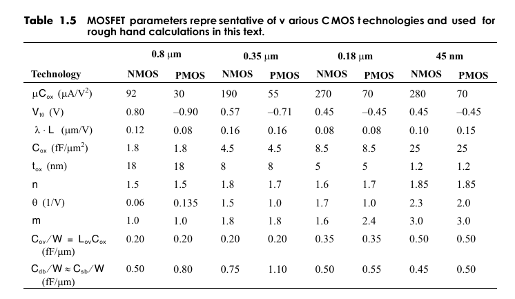
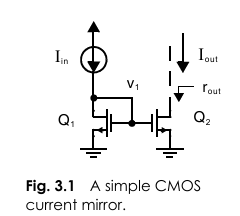
Give step-by-step solution with explanation and final answer:3.1 Consider the current mirror shown in Fig. 3.1, where I,, = 80 pA, transistor Q, has W/L = 100 pm/1.6 pm,
and transistor Q, has W/L = 25 um/ 1.6 pum. Find the nominal output current as well as the output resistance,
four Also, find the minimum output voltage such that both transistors remain in the active region. Use the NMOS
device parameters for the 0.8-um CMOS process in Table 1.5.
Table 1.5 MOSFET parameters repre sentative of v arious CMOS technologies and used for
rough hand calculations in this text.
0.8 um 0.35 um 0.18 um 45 nm
Technology NMOS pMOS NMOS pMOS NMOS pMOs NMOS PMOS
HC. (MAN?) 92 30 190 55 270 70 280 70
Vio (V) 080 090 057 071 045 045 045 045
aL (uv) 012 008 016 016 008 008 010 015
Cox (fF fun) 18 18 45 45 85 8.5 25 25
t,, (nm) 18 18 8 8 5 5 12 12
n 15 15 18 17 16 17 185 185
0 (V) 0.06 0135 15 10 17 10 23 20
m 10 10 18 18 16 24 30 30
Cu/W=1L,Co 020 020 020 020 035 035 050 050
(fF /um)
Ca/W=Cu/W 050 080 075 110 050 055 045 0.50
(fF /um)
I, 1 i Lu
v, |
lg Ton
a b a.
Fig. 3.1 A simple CMOS
current mirror.
Question:
Give step-by-step solution with explanation and final answer:3.1 Consider the current mirror shown in Fig. 3.1, where I,, = 80 pA, transistor Q, has W/L = 100 pm/1.6 pm,
and transistor Q, has W/L = 25 um/ 1.6 pum. Find the nominal output current as well as the output resistance,
four Also, find the minimum output voltage such that both transistors remain in the active region. Use the NMOS
device parameters for the 0.8-um CMOS process in Table 1.5.
Table 1.5 MOSFET parameters repre sentative of v arious CMOS technologies and used for
rough hand calculations in this text.
0.8 um 0.35 um 0.18 um 45 nm
Technology NMOS pMOS NMOS pMOS NMOS pMOs NMOS PMOS
HC. (MAN?) 92 30 190 55 270 70 280 70
Vio (V) 080 090 057 071 045 045 045 045
aL (uv) 012 008 016 016 008 008 010 015
Cox (fF fun) 18 18 45 45 85 8.5 25 25
t,, (nm) 18 18 8 8 5 5 12 12
n 15 15 18 17 16 17 185 185
0 (V) 0.06 0135 15 10 17 10 23 20
m 10 10 18 18 16 24 30 30
Cu/W=1L,Co 020 020 020 020 035 035 050 050
(fF /um)
Ca/W=Cu/W 050 080 075 110 050 055 045 0.50
(fF /um)
I, 1 i Lu
v, |
lg Ton
a b a.
Fig. 3.1 A simple CMOS
current mirror.
This is AI generated Response.
Asked by: M Murali
Created at: 2025-08-29 08:34:44
Final Answer:
RenderedRaw Text
Did you like this answer?
Let's solve the current mirror problem step by step:
---
## **Given Data**
- \( I_{in} = 80\, \mu A \)
- \( Q_1: \frac{W}{L} = \frac{100}{1.6} = 62.5 \)
- \( Q_2: \frac{W}{L} = \frac{25}{1.6} = 15.625 \)
- Use 0.8-μm NMOS process from Table 1.5:
- \( \mu C_{ox} = 92\, \mu A/V^2 \)
- \( V_{T0} = 0.80\, V \)
- \( \lambda \cdot L = 0.12\, (1/V) \cdot \mu m \implies \lambda = 0.12 / 1.6 = 0.075\, V^{-1} \)
---
## **Step 1: Nominal Output Current (\( I_{out} \))**
For a current mirror:
\[
I_{out} = I_{in} \times \frac{(W/L)_2}{(W/L)_1}
\]
Plug in the values:
\[
I_{out} = 80\, \mu A \times \frac{15.625}{62.5} = 80\, \mu A \times 0.25 = \boxed{20\, \mu A}
\]
---
## **Step 2: Output Resistance (\( r_{out} \))**
The output resistance is given by:
\[
r_{out} = \frac{1}{\lambda I_{out}}
\]
Recall:
\[
\lambda = \frac{0.12}{1.6} = 0.075\, V^{-1}
\]
So,
\[
r_{out} = \frac{1}{0.075 \times 20 \times 10^{-6}}
= \frac{1}{1.5 \times 10^{-6}}
= \boxed{666.7\, k\Omega}
\]
---
## **Step 3: Minimum Output Voltage (\( V_{out, min} \))**
For both transistors to remain in saturation (active region):
\[
V_{DS} \geq V_{GS} - V_{T}
\]
Find \( V_{GS} \) for \( Q_2 \):
The saturation current equation:
\[
I_{out} = \frac{1}{2} \mu C_{ox} \frac{W}{L} (V_{GS} - V_T)^2
\]
\[
20 \times 10^{-6} = \frac{1}{2} \times 92 \times 10^{-6} \times 15.625 \times (V_{GS} - 0.8)^2
\]
Calculate constant:
\[
\frac{1}{2} \times 92 \times 10^{-6} \times 15.625 = 0.00071875 \approx 7.19 \times 10^{-4}
\]
So,
\[
20 \times 10^{-6} = 7.19 \times 10^{-4} (V_{GS} - 0.8)^2
\]
\[
(V_{GS} - 0.8)^2 = \frac{20 \times 10^{-6}}{7.19 \times 10^{-4}}
= \frac{20}{719} \times 10^{-2}
= 0.0278
\]
\[
V_{GS} - 0.8 = \sqrt{0.0278} = 0.167
\]
\[
V_{GS} = 0.8 + 0.167 = 0.967\, V
\]
So,
\[
V_{out, min} = V_{GS} - V_T = 0.967 - 0.8 = \boxed{0.167\, V}
\]
---
## **Summary of Answers**
1. **Nominal Output Current (\( I_{out} \))**: \(\boxed{20\, \mu A}\)
2. **Output Resistance (\( r_{out} \))**: \(\boxed{666.7\, k\Omega}\)
3. **Minimum Output Voltage (\( V_{out, min} \))**: \(\boxed{0.167\, V}\)
Let me know if you'd like more details or derivations!
Question:
Give ME Each Step 100 Words Explanation only Theory
This is AI generated Response.
Asked by: M Murali
Created at: 2025-08-29 08:43:12
Final Answer:
RenderedRaw Text
Did you like this answer?
Certainly! Here's a concise, step-by-step explanation of each part with theoretical reasoning:
---
**Step 1: Calculating the Nominal Output Current**
In a current mirror, the output current is scaled from the reference current based on the ratio of the transistor widths and lengths. Assuming both transistors are identical in process parameters, the current ratio simplifies to the W/L ratio. Therefore, the output current equals the input current multiplied by the ratio of W/L of the output transistor to that of the reference transistor. This proportionality stems from the quadratic current equation in saturation, where the drain current depends on device geometry, enabling predictable current copying.
---
**Step 2: Determining the Output Resistance**
The output resistance of a MOSFET in saturation is primarily influenced by channel-length modulation, modeled by the parameter λ. It quantifies how the drain current varies with changes in drain-to-source voltage, effectively creating a finite output impedance. The resistance is inversely proportional to the product of λ and the drain current. This resistance impacts the current mirror's output impedance, affecting its ability to maintain a constant current under varying load voltages. The calculation reflects the device's physical channel-length modulation behavior, which depends on process parameters.
---
**Step 3: Finding the Minimum Output Voltage for Saturation**
A MOSFET remains in saturation when the drain-to-source voltage exceeds \((V_{GS} - V_T)\). To ensure both transistors stay active, the output voltage must be at least \(V_{DS} \geq V_{GS} - V_T\). Using the quadratic current equation, we solve for \(V_{GS}\) that produces the desired current. This \(V_{GS}\) then determines the minimum \(V_{out}\) to keep the output transistor in saturation. The calculation ensures the device operates in its active region, preventing cutoff or triode operation, which would compromise the current mirror's accuracy.
---
Let me know if you'd like further elaboration!
VIPSolutions focuses on clear, step‑by‑step explanations so you can learn quickly. Whether you need an AI‑generated walkthrough or a short hint to get unstuck, each solution is organized for fast reading and easy review later.
Search similar questions, compare approaches, and bookmark the best answers for revision. Our goal is simple: quick, reliable study help that feels natural—not noisy.
 VIPSolutions

 3.1 Consider the current mirror shown in Fig. 3.1, where I,, = 80 pA, transistor Q, has W/L = 100 pm/1.6 pm,
and transistor Q, has W/L = 25 um/ 1.6 pum. Find the nominal output current as well as the output resistance,
four Also, find the minimum output voltage such that both transistors remain in the active region. Use the NMOS
device parameters for the 0.8-um CMOS process in Table 1.5.
Table 1.5 MOSFET parameters repre sentative of v arious CMOS technologies and used for
rough hand calculations in this text.
0.8 um 0.35 um 0.18 um 45 nm
Technology NMOS pMOS NMOS pMOS NMOS pMOs NMOS PMOS
HC. (MAN?) 92 30 190 55 270 70 280 70
Vio (V) 080 090 057 071 045 045 045 045
aL (uv) 012 008 016 016 008 008 010 015
Cox (fF fun) 18 18 45 45 85 8.5 25 25
t,, (nm) 18 18 8 8 5 5 12 12
n 15 15 18 17 16 17 185 185
0 (V) 0.06 0135 15 10 17 10 23 20
m 10 10 18 18 16 24 30 30
Cu/W=1L,Co 020 020 020 020 035 035 050 050
(fF /um)
Ca/W=Cu/W 050 080 075 110 050 055 045 0.50
(fF /um)
I, 1 i Lu
v, |
lg Ton
a b a.
Fig. 3.1 A simple CMOS
current mirror.