This is AI generated Response.
Asked by: Prasanna Manda
Created at: 2025-09-27 20:02:25
Final Answer:
RenderedRaw Text
Did you like this answer?
Let's break down the problem based on the images and data provided.
---
## 1. **Circuit and Parameters**
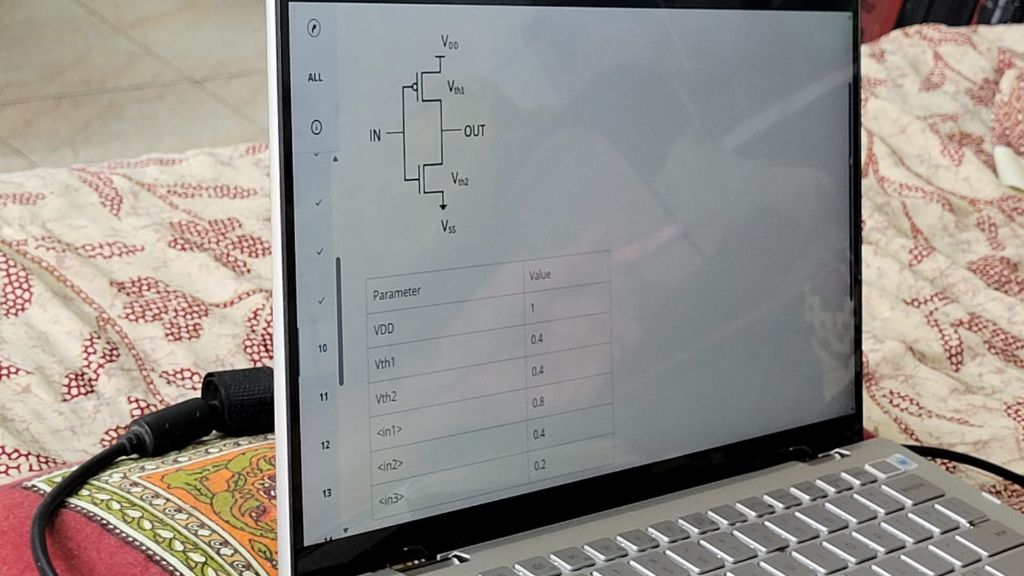
From the **first image**:
- You have a CMOS inverter circuit (one PMOS on top, one NMOS at the bottom).
- The table lists the following values:
- **VDD** = 1 V
- **V1** (PMOS threshold) = .4 V
- **Vth2** (NMOS threshold) = .4 V
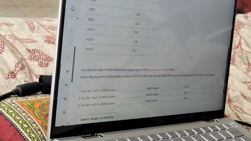
- **<in1>** = .8 V
- **<in2>** = .4 V
- **<in3>** = .2 V
---
## 2. **Transistor States Explanation**
### **NMOS (bottom transistor)**
- **Turns ON** (conducts) when **V<sub>IN</sub> > Vth2**
- **Turns OFF** when **V<sub>IN</sub> < Vth2**
### **PMOS (top transistor)**
- **Turns ON** (conducts) when **V<sub>IN</sub> < (VDD - |Vth1|)**
- **Turns OFF** when **V<sub>IN</sub> > (VDD - |Vth1|)**
For VDD = 1 V, Vth1 = .4 V:
- PMOS ON if **V<sub>IN</sub> < .6 V**
---
## 3. **Evaluating Each Input**
### **(a) For IN = <in1> = .8V**
- **NMOS:** .8V > .4V ⇒ **ON (Saturation/Active)**
- **PMOS:** .8V > .6V ⇒ **OFF**
- **OUT:** Pulled **LOW** (V, VSS)
### **(b) For IN = <in2> = .4V**
- **NMOS:** .4V = .4V ⇒ **Just at threshold, assume ON (Saturation)**
- **PMOS:** .4V < .6V ⇒ **ON (Saturation/Active)**
- **OUT:** Both transistors ON, **undefined/unknown** (could be somewhere between HIGH and LOW, but in practice, it's a transition region).
### **(c) For IN = <in3> = .2V**
- **NMOS:** .2V < .4V ⇒ **OFF**
- **PMOS:** .2V < .6V ⇒ **ON (Saturation/Active)**
- **OUT:** Pulled **HIGH** (1V, VDD)
---
## 4. **Summary Table**
| IN | PMOS State | NMOS State | OUT |
|-------|------------|------------|---------|
| .8 V | OFF | ON | LOW (V)|
| .4 V | ON | ON | Unknown |
| .2 V | ON | OFF | HIGH (1V)|
---
## 5. **Brief Explanation**
- When **IN is high (.8V)**: NMOS is ON, PMOS is OFF, output is LOW.
- When **IN is low (.2V)**: NMOS is OFF, PMOS is ON, output is HIGH.
- When **IN is at threshold (.4V)**: Both transistors are ON, output is undefined (may be between HIGH and LOW).
---
### **How to Fill the Blanks in Your Question**
- For IN=<in1> (.8V): PMOS state = OFF, NMOS state = SATURATION, OUT = V
- For IN=<in2> (.4V): PMOS state = SATURATION, NMOS state = SATURATION, OUT = UNKNOWN
- For IN=<in3> (.2V): PMOS state = SATURATION, NMOS state = OFF, OUT = 1V
---
Let me know if you need further clarification!
VIPSolutions focuses on clear, step‑by‑step explanations so you can learn quickly. Whether you need an AI‑generated walkthrough or a short hint to get unstuck, each solution is organized for fast reading and easy review later.
Search similar questions, compare approaches, and bookmark the best answers for revision. Our goal is simple: quick, reliable study help that feels natural—not noisy.
 VIPSolutions
 . J
i
BP
| i a
(0) out :
IN ons T&F
| BE i Ate
BN A)
: ‘a | >
Sn Vs EAN
- FAN AT 2)
Bhs. al | & ay
STR fr J | po
or he. SRR es) parameter Pe
222d Tara v : or
J NG AE | ads
ANE v u | rds
\ 4 w En
2S To SE vit = RONG
Sau 2 '@
# CL " vin? s Cae A
ts a> Po J
2! i= g— NS 3
SSeS x Sh aN NONI
ES (Ge Si = _ ea >= =
Bo NT NG a > OB 4 —
¥ BR aA - pp DN EAT
BR ORR = rea >3 ENON
Sh CONTE a > BR SES SY TN
| °F ph]
| = |
I vl :
© vm | f
J v
- N 31% ro = |
. 2 Snag 04 |
H v y
te Ha she 02 ”
REE LTTR v :
SE HELEN EEE
Eo AY
TER Describe the state of PMOSINMOS 3nd output m A :
A R. 10 5 and output signal OUT) for exh rp below oy
> £5 (Note: Represent the PMOS3/NMOS states as (OFF, SATURATION] and use UNKNOWN forany: the banks becw f heres 8 ct looms | €
i ee
GA) 1. For IN= V, PMOS state NOs ste ours v -
8 == a oN on v ;
rE : EL io Mosse ! \
EE 1 als i Foi are 2
SG 3 Fore