 VIPSolutions
>... SELON a AN By AANA vi 05 ana = 06 oe 2iosEE7 Cre
Question:
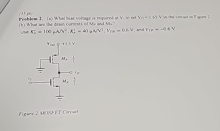 >...
SELON
a AN By AANA vi 05 ana = 06
oe 2iosEE7 Cre
This is AI generated Response.
Asked by: Adapaka Jagadeesh
Created at: 2025-11-21 22:45:38
Asked by: Adapaka Jagadeesh
Created at: 2025-11-21 22:45:38
Final Answer:
Rendered
Raw Text
Did you like this answer?
# Solution toFET Circuit Problem
Let’s break down the steps for solving the given problem:
---
## **Given Data**
- \( K_{p}' = 100~\mu\text{A}/V^2 \) (for PMOS, \( M_P \))
- \( K_{n}' = 40~\mu\text{A}/V^2 \) (for NMOS, \( M_N \))
- \( V_{TN} = .6~V \) (NMOS threshold)
- \( V_{TP} = -.6~V \) (PMOS threshold)
- \( V_{DD} = 3.3~V \)
- \( V_O = 1.65~V \) (desired output)
---
## (a) **What bias voltage is required at \( V_{I} \) to set \( V_{O} = 1.65~V \)?**
### **Step 1: Node Voltages**
- Source of \( M_P \): \( V_{DD} = 3.3~V \)
- Source of \( M_N \): Ground = \( ~V \)
- Drain of both (node \( V_O \)): \( 1.65~V \)
### **Step 2: Gate-Source Voltages**
Let \( V_G \) be the gate voltage for both transistors (since both gates are tied together).
- For \( M_P \) (PMOS, top transistor):
- Source: \( 3.3~V \)
- Gate: \( V_I \)
- \( V_{SGP} = V_{S} - V_{G} = 3.3 - V_I \)
- For \( M_N \) (NMOS, bottom transistor):
- Source: \( ~V \)
- Gate: \( V_I \)
- \( V_{GSN} = V_I - = V_I \)
---
### **Step 3: Currents (In Saturation)**
For both, the currents must be equal: \( I_{DP} = I_{DN} \).
#### **NMOS:**
\[
I_{DN} = K_n (V_{GSN} - V_{TN})^2 = 40~\mu\text{A}/V^2 \cdot (V_I - .6)^2
\]
#### **PMOS:**
\[
I_{DP} = K_p (V_{SGP} - |V_{TP}|)^2 = 100~\mu\text{A}/V^2 \cdot (3.3 - V_I - .6)^2
\]
Set equal:
\[
100 (2.7 - V_I)^2 = 40 (V_I - .6)^2
\]
---
### **Step 4: Solve for \( V_I \)**
\[
\frac{100}{40} (2.7 - V_I)^2 = (V_I - .6)^2
\]
\[
2.5 (2.7 - V_I) = V_I - .6
\]
\[
2.5 \cdot 2.7 - 2.5 V_I = V_I - .6
\]
\[
6.75 - 2.5 V_I = V_I - .6
\]
\[
6.75 + .6 = V_I + 2.5 V_I
\]
\[
7.35 = 3.5 V_I
\]
\[
V_I = \frac{7.35}{3.5} \approx 2.10~V
\]
---
## (b) **What are the drain currents of \( M_P \) and \( M_N \)?**
Plug \( V_I = 2.10~V \) into either current equation:
\[
I_D = 40~\mu\text{A}/V^2 \cdot (2.10 - .6)^2 = 40~\mu\text{A}/V^2 \cdot (1.5)^2 = 40 \cdot 2.25 = 90~\mu\text{A}
\]
---
## **Final Answers**
### **(a) Bias voltage at \( V_I \):**
\[
\boxed{2.10~V}
\]
### **(b) Drain currents of \( M_P \) and \( M_N \):**
\[
\boxed{90~\mu\text{A}}
\]
---
**Summary Table:**
| Parameter | Value |
|---|---|
| \( V_I \) | 2.10 V |
| \( I_{DP} = I_{DN} \) | 90 μA |
---
**Figure 2 MOSFET Circuit**
*The calculations above apply to the circuit shown in the image.*
📢 Instructions:
- Ask anything relatd to above question only.
- For new Question goto :